PCBway - Part 1 : Linear amplifier project part 6
 |
| PCBWay supplied the PCBs for this project as part of a collaboration — my write-up here is focused on the technical aspects of the design and build. |
In the amplifier project, I need to measure currents and voltages. Plate voltage (Ua), plate current (Ia), screen voltage (Ug2), screen current (Ig2), control grid current (Ig1) and also control grid voltage (Ug1).
My first approach failed due to me not thinking properly. The current measuring relies on shunt resistors, which is a proven and reliable way to measure dc current. A resistor is placed in a branch of the power supply and by measuring the voltage drop across the resistor we can calculate the current, using ohms law, I=U/R.
Upon testing the amplifier I realised that the arduino would not measure any current. Voltage measurment (Ua, Ug2) uses voltage dividers, and that worked as planned. Eventually it dawned upon me that I was trying to read a negative voltage as seen from the reference plane (chassis ground) with the arduino. In short, all the current flows from it's supplies (plate, screen), through the tubes, and since the cathodes of the tubes are directly grounded to chassis, it flows through the chassis, back to each supply, causing a negative potential between chassis and the top of the shunt resistors facing the negative side of the supply. The control grid operates a little different. When the control grid starts drawing current, it flows from the grid to ground, causing a positive potential on top of the shunt resistor as seen from chassis.
Arduinos does not like negative voltage on it's analog pins, and the way I had set things up did not work so I needed a fix.
 |
| Here I have tried to illustrate the current flow in the amplifier. Note that since the arduino tried to read a negative voltage, it won´t work. |
Alternatives
I could have run an isolated line from the cathodes to the negative terminal of the plate supply (that's what I've done in my dual 813 GG amp), with an inline shunt. That works for grounded grid, with a separate, floating meter, but not for single ended metering like I'm doing with the arduino. It would also be hard to differ screen from plate current with an isolated B- and single ended measuring.
I could implement some kind of differential measurment. I guess there are IC's ready to do just that, but that felt a bit overkill, since I had a somewhat working system already (using a DMM across the shunts, I could measure the voltage developed across them, and calculate currents), and I did not feel like rebuilding a lot of stuff
 |
| Inverting Opamp schematic and formula |
I settled on inverting amplifiers using the old LM358 operational amplifier. This changes the input from negative to positive, or the other way around. As a bonus, I could adjust the gain to suit the 10bit ADC of the arduino better and get better resolution. For example, control grid current is very small, (it should be 0 for class AB1), but I still wanted to measure it's presence, but I did not want to introduce a high resistance in the dc path of the supply with a higher value shunt resistor (remember, higher value shunt gives higher voltage across it for a given current flow).
Time to get to work
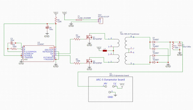
As it happened, Emily from PCBWay reached out to me asking if I was interested in doing a collaboration. She had seen some of my previous work here on the blog. PCBWay would supply boards, I would do a writeup about it. Sure, why not. Having only used JLCPCB before, I figured it would be good to widen the horizons. I did not have any fancy designs waiting to be sent out for fabricating but I had a few in mind, amongst others this LM358 inverting amplifier with power supply. Over the years of fixing up old radios, I have also had the need for "universal" rectifier pcb's, A serious voltage divider for HV measuring was also things I could think of that I needed. I was very grateful that they sponsored a bunch of boards! More on that in my next post.
The opamp inverter

To shift the negative voltage developed over the shunt, a dual power supply opamp is needed. Initially, it felt like a pain having to build a dual rail power supply, possibly stabilised, but as I learnt, there was no need to stabilize it, for one, the current draw is miniscule, and , since the output only mirrors the input, as long as I kept the VCC and VDD well above and below the wanted signal I shouldn't have any issues in case of voltage drop. I found a pcb mount transformer from one of my donor boards (never throw something away), which had dual 9 V, 2.5 VA secondaries, which suited me perfect (actual measured voltage after rectification shows +-16 V). I measured and made a footprint in kicad and incorporated that in the design.
I decided to make three inverting channels, and one non-inverting channel. The inverting channels is to be used with plate and screen current measurments and voltage measurment of the control grid bias (which is a negative voltage). The non-inverting channel is to be used to measure control grid current.
I laid out the board with dual footprints for the LM358, in DIP-8 and VSSOP-8 since I had both variants at home. I made the DIP-8 surface mount as well, since I have adopted that when etching boards at home. That way there are less holes to drill, and it´s easier to replace a damaged component.
Gain is set at 1 for plate current, 4.7 for screen current, and 10 for control grid current. For voltage measurment, the gain is set at 1. To protect the analog in pins of the arduino, TVS diodes are installed on the output channels of the board.

Ordering with PCBway was easy and straight forward, with a layout similar to other hobby pcb manufacturers. Upload your gerber, choose how many boards you want, thickness etc, put it in your cart and check out. PCBway had a nice progress bar you can follow, with videos showing each of the manufacturing steps. I chose Fedex shipping and the boards arrived quickly and well packed.

I made some small adapter boards for the position feedback potentiometers, and I was happy to see that they had made 5 extra boards.
Testing the inverter.
 |
| Finished board, tested and ready to be installed in the logic chassis |
Testing
I applied AC (watch your fingers) to the transformer primary, and applied a negative voltage on the inverting input ports, one by one, measuring the output. I'm happy with the linearity on all channels.

For example, channel 1, with unity gain (1), -0,118 V in, gave 0.12 V out. -1.181 gave 1.184V out, This could be improved with offsets and biasing, but lets be honest. It´s good enough for what I´m after.
Now it´s just the case of installing it in the logic chassis and to wire it up.
For custom utility boards like this (simple analog interfaces), PCBWay’s standard service was straightforward and delivered boards that worked as expected!
More to come
73


Comments
Post a Comment